

MAASTEK TECHNOLOGIES
(A Unit of MAASTEK Research and Consultancy Services, Jaipur)
Deep-tech engineering from India. Serving defense, industrial, and research customers across RF, plasma, and embedded systems
Precision RF/Microwave
& Prototype PCB
ENGINEERING EXCELLENCE
From concept to fabricated prototype — MAASTEK Technologies delivers high-performance RF/Microwave systems, SMPS & LED drivers, plasma-based solutions, IoT modules, and MPCVD diamond growth consultancy for industrial & academic clients worldwide.

⬇️ SCROLL TO EXPLORE
13 + Years of Experience
Highly Experienced Team
Advance Facilities
Excellent Services
What We Do
Core Services
End-to-end design, full-wave simulation, and in-house fabrication for RF, microwave, plasma, and electronics applications.

Prototype PCB Fabrication
In-house fabrication of RF/microwave and mixed-signal PCBs. From schematic to tested prototype using high-frequency substrates — Rogers, PTFE, FR4 — with precision metallization and SMD assembly.

SMPS & LED Driver Design
Switch-mode power supply and LED driver design from specification to verified hardware. PWM based topologies, isolated flyback, multi-rail designs with full LTspice simulation and thermal analysis.
.png)
RF/Microwave Device Design
Full-spectrum RF front-end design. EM simulation in appropriate available platforms. LNA, PA, directional couplers, power detectors, Filters, Power Divider/Splitter, Match Load, Switch Bank Filter, wideband AGC systems, and antennas.
.png)
Plasma Applications & MPCVD Consultancy
APPJ surface activation (2.45 GHz, 50W GaN), DBD plasma systems, plasma-activated water, and MPCVD reactor consultancy for lab-grown diamond. COMSOL-coupled plasma simulation with full SOP documentation. Polycrystalline diamond wafer development and recipe preparation. GaN on Diamond Process and development.
Industrial & Academic RF Projects
Custom RF/microwave solutions for agriculture, textile, pharma, and academia. Microwave soil moisture sensing, food processing, wearable diagnostics, plasma-activated water (PAW), agri-waste pyrolysis, and RFID traceability. Customised designs on request.
.png)
IoT & Telecom Module Design
ESP32-based IoT systems with multi-sensor integration — ZMPT101B, BMP280, ACS712, HC-SR04, LDR — isolated multi-rail power architectures, and telecom module design with full firmware and hardware delivery.
WHO WE ARE
Movers &
Shakers in
Microwave Tech
"We build what others only simulate — from PCB prototype to plasma reactor."
MAASTEK Technologies was founded by a group of 3 engineering graduates, They are PhD-qualified in RF/Microwave Engineer, and Signal Processing. Also Senior IEEE Member with over 13 years of combined academic and industrial experience spanning MNIT Jaipur, SP3 Technologies, TATA Consumer Products, and multiple academic institutions.
We provide innovative, high-performance RF/Microwave components, front-end devices, advanced SMPS/LED drivers, and plasma-based industrial systems — from prototype fabrication to full-scale deployment. Based in Rajasthan with direct reach into Gujarat's industrial clusters.
TECHNICAL CAPABILITIES
-
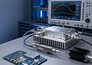
Full EM simulation stack: (Appropriate EM/Multiphysics Platform) with parametric sweep and optimization workflows
-
In-house PCB fabrication for RF/microwave substrates — Rogers, PTFE, high-frequency FR4
-
Seki SDS 6K MPCVD reactor operation (2.45 GHz, 6 kW) — PCD and SCD growth with recipe development
-
Wideband RF front-end design: 0.4–6 GHz, AGC, log power detectors (AD8318, LT5537), directional couplers, Power Amplifiers, Antenna, Switch Bank filters.
-
APPJ plasma surface activation system: 2.45 GHz, 50W GaN PA with plasma simulation and full scale device development
-
H-terminated diamond gas sensor development — interdigitated electrodes, Ti/Au metallization, NO₂/NH₃/O₃ detection
-
Multi-rail isolated flyback PSU design (12V/5V/3.3V)/ LED Drivers and Industrial Power Supplies with LTspice simulation
-
ISO-quality SOP documentation and engineering process development for plasma and RF systems